The structure of the conventional single layer capacitor is that metal electrodes are printed on the upper and lower surfaces of the ceramic dielectric layer to form a common parallel plate capacitor structure, so as to obtain the corresponding capacitance value. Due to the structure is limited by the size of the capacitor and the dielectric properties of the ceramic material (including dielectric constant, temperature characteristics, etc.), when the overall size and the ceramic material used are determined, the capacitance value is fixed. Therefore, in many application scenarios, the assembly space is limited, and the overall size of the chip capacitor is fixed. If the conventional single layer capacitor is used, it is easy to appear that the actual capacitance value is less than the capacitance value required by the application.
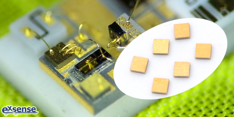
In order to solve the above problems, EXSENSE Electronics introduces a single layer capacitor that can not only meet the size requirements, but also effectively increase the capacitance value. Its capacitance value is much higher than that of conventional single layer capacitor with the same ceramic material and overall size. The chip capacitor has an internal interconnection structure, including the ceramic dielectric layer, the inner electrode and the outer electrode. The ceramic dielectric layer contains two relatively established inner electrodes, and the upper and lower surfaces are provided with outer electrodes. The outer electrode is electrically interconnected with the inner electrode through an interconnect hole arranged on the ceramic dielectric layer. The preparation method is as follows:
First, the upper ceramic substrate, the lower ceramic substrate and the middle ceramic substrate are prepared by stacking and prepressing the raw ceramic material after tap casting;
Second, the surface of the upper ceramic substrate and the lower ceramic substrate is covered with blue tape, and the holes are drilled respectively to get through the interconnect holes; The middle ceramic substrate is drilled to obtain the positioning hole, then the interconnect holes of the upper ceramic substrate and the lower ceramic substrate are metallized and filled, and the blue tape is removed;
Third, the inner electrode is printed on one side of the upper ceramic substrate and the lower ceramic substrate respectively;
Fourth, the lower ceramic substrate is placed on the lower laminate, stack the middle ceramic substrate, the upper ceramic substrate, the upper laminate on the lower ceramic substrate, stacking when the printed side of the inner electrode is facing inward, then laminated, laminated products sintered to get the ceramic dielectric layer;
Fifth, metal electrodes are printed on the upper and lower surfaces of the ceramic dielectric layer by sputtering or coating process to obtain single layer capacitor with internal interconnect structure.
This single layer capacitor increases the internal electrode, chip capacitor with large capacitance value can be obtained due to small spacing. Through the interconnect holes in the upper and lower ceramic dielectric layers, the internal and external electrodes are connected electrically, so as to ensure the overall size of the capacitor. Compared with the conventional single layer capacitor, this chip capacitor has the advantages of simple structure, high reliability and superior performance.