Single layer capacitor produced by EXSENSE Electronics Technology Co., Ltd. has characteristics of small size, strong structure, great frequency characteristics etc., which is widely used in microwave communication lines and anti-electro magnetic interference (EMI) devices. Compared with multi-layer ceramic capacitors (MLCC), single layer capacitor has the advantages of low equivalent series resistance, low dielectric loss and high reliability.
The basic structure of the single layer capacitor is the metal electrode -ceramic dielectric substrate -metal electrode. Its conventional preparation process is: tape casting→lamination→bar cutting→adhesive discharging→sintering→sputtering→electroplating→dicing. Among them, dicing generally adopts mechanical cutting method, such as rotary blade cutting. However, due to the ceramic material is brittle, the cutting surface of ceramic substrate is easy to break when cutting, which is not conducive to the structural integrity and reliability of capacitor. Based on this, EXSENSE Electronics introduces a low-stress single layer capacitor, which ceramic substrate cutting surface is not easy to crack, which has the characteristics of good structural integrity and great reliability.
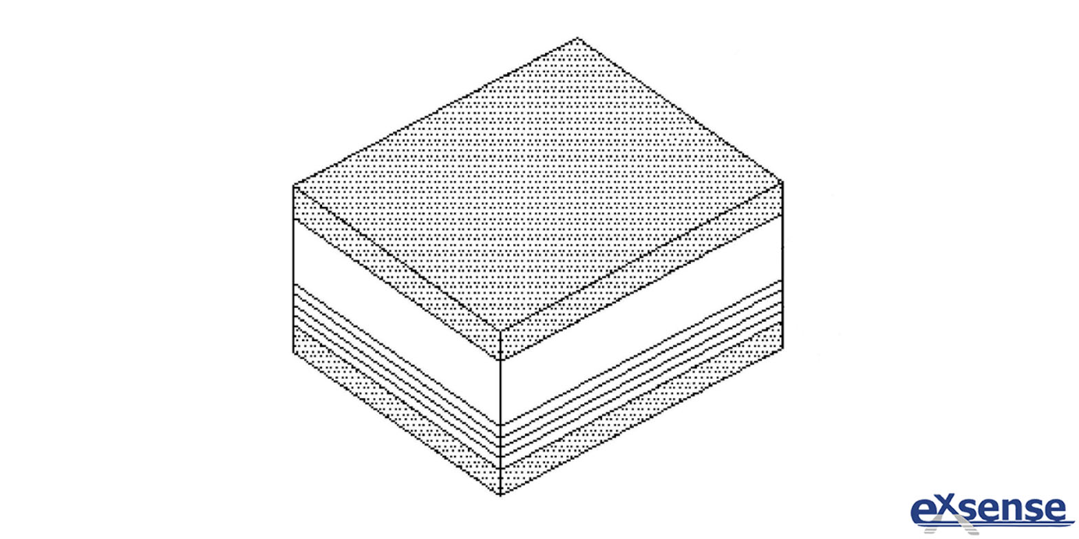
Low-stress single layer capacitor comprises a ceramic substrate, surface electrode, bottom electrode and at least one buffer layer located inside the ceramic substrate. The surface electrode is arranged on the top surface of the ceramic substrate; The bottom electrode is arranged on the bottom surface of the ceramic substrate; The buffer layers are spaced perpendicular to the bottom surface of the ceramic substrate, which is a hollow metal layer with a closed frame shape and the frame is arranged along the side of the ceramic substrate and exposed to the side surface of the ceramic substrate. The buffer layer can reduce the influence of cutting stress on the cutting surface of ceramic substrate and avoid the fragmentation of the cutting surface, so as to keep the whole structure of single layer capacitor intact and ensure the performance and reliability of single layer capacitor. At the same time, by setting at least one metal layer at least one interval, the cutting stress can be dispersed and the effect of preventing fragmentation is better. The preparation method of low-stress single layer capacitance is as following:
First, the ceramic slurry is made into ceramic film by the tape casting method.
Ceramic slurry can be used by the industry with ceramic powder preparation technology, ceramic powder can be used capacitance ceramic withⅠclass porcelain, Ⅱporcelain or Ⅲ porcelain powder; The thickness of the ceramic film is 5~60 micron.
Second, the surface of ceramic film made of metal slurry in step First is printed with a number of closed frame-shaped buffer layers.
The metal slurry can be silver, palladium, silver-palladium alloy, nickel, copper, nickel-copper alloy, etc., the preference is to choose the metal slurry which can be co-fired with the ceramic film prepared in step First. The screen printing method is adopted to print the buffer layer, and the buffer layer is crisscrossed with grid network. The thickness of the buffer layer is 0.5~3 micron.
Third, the ceramic slurry prepared in step First is laminated with at least one ceramic film obtained in step Second, so as to obtain the raw ceramic bars at the bottom of each buffer layer.
Firstly, four ceramic films obtained in step Second is laminated together, and the buffer layer on the four ceramic films is separated from each other. Then, the ceramic films produced by step First is laminated on the exposed buffer layer until the required thickness of the chip capacitor is reached. The spacing between the two adjacent buffer layers in the raw ceramic bars is equal and is 5~ 20 microns.
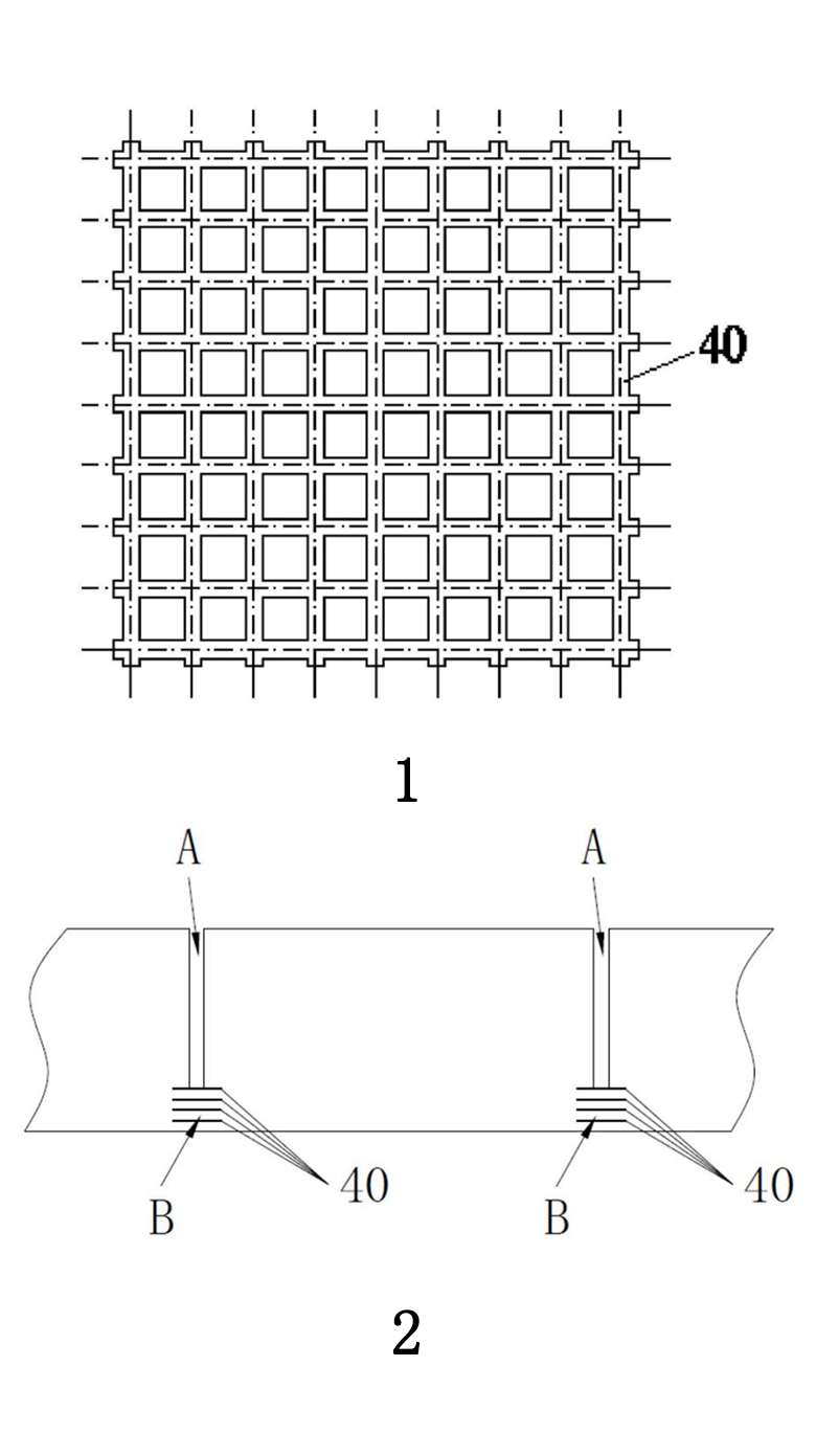
Fourth, raw ceramic bars of step Third are cut into smaller size, then from top bottom cut the small raw ceramic bars into groove along the border line of buffer layer, as shown in figure 1, the dotted line is the cutting line, and the bottom of the groove A included reserved part B of buffer layer 40, the reserved part B does not cut off, as shown in figure 2.
Fifth, the semi-finished products obtained in step Fourth are adhesive discharged and sintered.
The semi-finished products obtained in step Fourth are adhesive discharged in air at 250~400℃ to ensure the uniform density of the sintered ceramics.The semi-finished products are sintered at 900~1350℃ in air or reducing atmosphere after adhesive discharged.
Sixth, surface electrode and bottom electrode are made on the top surface and bottom surface of semi-finished products respectively.
The surface electrode and the bottom electrode are made by sputtering or electroplating method. The materials can be at least one metal of titanium, tungsten, platinum, cobalt, copper, nickel, palladium, gold and tin or any combination of alloys. The thickness of the surface electrode and the bottom electrode are respectively 2 microns.
Seventh, the semi-finished products obtained in step Sixth are cut through the groove, and the reserved part B is cut off to obtain a single low-stress single layer capacitor.
In the preparation method of low-stress single layer chip capacitor, the ceramic film obtained by step First tape casting method has a large area, which is inconvenient for subsequent treatment. Therefore, in step Fourth, the use of the plasticity of the ceramic bar, the first ceramic bar is cut into smaller pieces, and the obtained ceramic bar is pre-cut into groove, so after lamination of its cutting and pre-cutting will not produce fragmentation. After completing step Fifth and step Sixth, in step Seventh to cut reserve department, while cutting object is the brittle ceramic clinker, but due to the reserved part contains the buffer cutting stress buffer layer, so cut off to prevent fracture, and compared with the existing technology, greatly reduced the cutting thickness of ceramic clinker, which is more effective to prevent fracture of the cutting surface.